Yundoo Y8 RK3399 Settop Box (Part 2)

Debug-UART

Although the Y8 has no pin header providing access to the Debug UART, its easy to add one, given you have a soldering iron at hand:


As the pads have a 2.0 mm spacing, I used a short piece of ribbon cable with the typical 2.54 mm pin header at the other end. The RK3399 UART uses 1.5 Mbps instead of the common 115.2 kbps.

MaskRom Mode

The RK3399 has a fixed boot order – SPI, eMMC, SD card. So to force the RK3399 to boot anything different than the Android firmware on the internal, soldered eMMC flash, one has to „disable“ the eMMC. The canonical method for doing so on any Rockchip board is to short the eMMC clock line to ground. As the bootrom code can no longer detect any usable boot code on the eMMC it will try the SD card next and will finally fall back the so called MaskRom mode. The MaskRom code provides access to the SoC via USB, allowing to bootstrap the device.

Finding the eMMC clock was a little bit more difficult – the eMMC chip is a BGA chip on the top of the PCB. Older NAND chips in TSSOP packages allowed to directly access the the chip pins, obviously this is not possible with BGAs. As there are no PCB traces near the eMMC on the top layer, there was a quite good chance to find the relevant traces on the bottom layer. Two photos and a few minutes later, spend with GIMP to to carefully align the two images, I was able to locate the traces and a few test points:

From the datasheet of the Samsung KLMBG4WEBD-B031 eMMC flash it became apparent the clock had to be on the left side of the board. Using my scope I measured the signals available on the different test points, et voilà, found a steady 200 MHz signal. Another give away was the 22 Ω resistor on this signal, which can also be found in the Firefly-RK3399 schematics.


The series resistor is somewhat odd, as a series resistor for signal conditioning should normally be located near the driver (i.e. the SoC). Anyway, it makes a nice spot to force the clock signal to ground.

When pressing the Power button to start the Y8, normally the red LED lights up for one to two seconds and then becomes blue. When the eMMC clock is shorted, the LED will stay red, and the device is in MaskRom mode. The Y8 can be connected to a USB host using a  USB Type-C to Type-A cable, and it will show up with the RK3399 specific Vendor/Product ID 2207:330C.

To be continued …

Yundoo Y8 RK3399 Settop Box (Part 1)

For some tasks like compiling and QA tests I was looking for some more powerful additions to my SBC collection of RPI3 and Allwinner Pine64. Requirements: Aarch64, plenty of RAM, fast CPU, fast network, mainline kernel support (in a not to distant future).

Currently, many SBCs available in the 100 $US/€ price range only have 1 or 2 GByte of RAM (or even less) and often provide just 4 Cortex-A53 cores running at 1.2-1.4 GHz. There are some exceptions, at least regarding the CPU power, but still limited memory (some examples):

  • BananaPi M3 (85€)
    • Pros: 8 Cores @ 1.8 GHz (Allwinner A83T), GBit Ethernet, 8 GByte eMMC
    • Cons: ARM A7 (32bit), 2 GByte RAM, only 2x USB 2.0, PowerVR graphics
  • LeMaker HiKey 620 (109 $US)
    • Pros: 8 Cores @ 1.2 GHz (Kirin 620), 64bit (A53) 8 GByte eMMC
    • Cons: No ethernet, 2 GByte RAM, only 3x USB 2.0, discontinued
  • Asus Tinkerboard (65€)
    • Pros: 4 Cores @ 2.0 GHz (Rockchip RK3288), GBit Ethernet
    • Cons: ARM A17 (32bit), 2GByte RAM, USB 2.0 only (4x)

There are more expensive options like the LeMaker HiKey 960 (240€, 3 GByte RAM, still no ethernet), or the Firefly RK3399 (200€, 4 GByte RAM), but these where clearly out of the 100€ price range.

The SBC board all sport a considerable number of of GPIOs, SPI and I2C ports and the like, but for hardware connectivity I already have the above mentioned bunch of RPIs (1 and 3) and Pine64 boards. So going into a slightly different direction, I investigated some current settop boxes.

Rockchip RK3399

The Rockchip RK3399 used on the Firefly is one of the available options, itt powers several different STBs with different RAM and eMMC configurations. I went with the the Yundoo Y8, for the following reasons:

  • 4 GByte of RAM
  • 32 GByte of eMMC
  • 2 A72 Cores (2.0 GHz) + 4 A53 Cores (1.5 GHz)
  • 1x GBit Ethernet
  • 1x USB 3.0, standard A type receptable
  • 1x USB 3.0, Type C (also provides DisplayPort video using alternate mode)
  • 2x USB 2.0, Type A
  • available for 105€, including EU power supply, IR Remote, short HDMI cable

Contrary to the above mentioned Firefly, you neither get PCIe expansion ports nor any GPIOs, so if this is a requirement the Y8 is no option for you.

In the next part, I will give some more details useful for running stock Linux instead of the provided Android 6.0 on the device – so stay tuned for UART info, MaskRom mode etc.

Update: UART/MaskRom info is now available: Yundoo Y8 RK3399 Settop Box (Part 2)

TinyBoy2 firmware upgrade to Marlin 1.1.0-RC8/RCBugFix

The TinyBoy2 is a Indiegogo backed 3d printer. On the plus side, it is very small (16×18 cm² desk space), and it does it jobs.

Like a lot of crowd funded projects, there is essentially no after campaign support. The firmware is a hacked version of Marlin 1.1.0-RC3. The code for the firmware which is shipped with the hardware is supplied as a code drop, but there is no changelog, and the diff to the upstream RC3 contains a lot of awkward changes, e.g. changes to the display SPI code, although the TB2 display uses I₂C. The diff between the code drop and RC3 is 53 files changed, 2196 lines removed, 2072 lines added.

As I wanted to update my printer to a recent firmware (RC3 was tagged December 2015) to get all the new features and bugfixes, and also to change the FW behaviour, I started with the current Marlin GIT, and added the necessary changes on top.

The nice part is that current Marlin is completely capable to drive the printer, support is mostly added by creating a suitable Configuration and setting the right pins for steppers, PWM, encoder and so on. The changes have been submitted upstream, or you can just pull the patched tree from my Marlin github repo.

Download the compiled firmware

In case you do not want to compile the FW yourself, I have prepared 4 variants: L10/L16, both with and without heatbed support:

Firmware-Download

-----BEGIN PGP SIGNED MESSAGE-----
Hash: SHA1

bd1af0b14e81c344d5ecac27a7c8ba09aaa96a0c  Marlin_TB2_L10_HeatBed.hex
fd754b2b9f0ff7271eb53c9cc9f022eee1b247b8  Marlin_TB2_L10.hex
f330e4ec2a3fcc32510c15b8f9c776731aa98598  Marlin_TB2_L16_HeatBed.hex
cc239598f0fe9ba0ccccb31b007c896c1595dea9  Marlin_TB2_L16.hex
-----BEGIN PGP SIGNATURE-----

iF0EARECAB0WIQSwWRWIpJbl0W4DemNvf0o9jP6qUwUCWM3KjQAKCRBvf0o9jP6q
U4HkAJ9GOBOmfTw1XUSQlTs745P7qKvO2wCfY/xWHpbGTfzuS7GZLDvTPnEjc7I=
=ce7+
-----END PGP SIGNATURE----

Flashing the firmware

Although it is possible to use Arduino to flash the firmware, I consider it much to bloated for the task, and as it uses avrdude behind the curtains, I prefer to call avrdude directly:

Backup shipped FW (sorry, not verified):

avrdude -p m1284p -b 57600 -c arduino -P /dev/ttyUSB0 -U flash:r:Backup.hex:i

Update to new FW:

avrdude -p m1284p -b 57600 -c arduino -P /dev/ttyUSB0 -U flash:w:Marlin.hex

(Update 2017-03-19 18:49 UTC: Added flashing paragraph)

MyGica T230C hacking

As DVB-T(1) is phased out in Germany soon, I got me a new DVB-T2 stick. The MyGica T230 is supported under Linux, and has a quite low price (~20€).

Instead of the expected T230, I received a T230C which has silently replaced the T230. The T230C is – although quite similar to the T230 – currently (Linux 4.10rc2) not supported by the mainline kernel.

Compared to the T230, the T230C uses the same Cypress FX2 CY7C68013A USB bridge chip, a Silabs Si2168-D60 demodulator (new revision) and a new tuner chip, Silabs Si2141-A10 (T230 uses a Si2157).

img_0419_v1img_0420_v1
img_0440img_0429
img_0429_440_overlay

Beyond the bridge/RF chips, there is an I2C eeprom (FX2 firmware?), two LowPowerSemi adjustable, synchronous DC/DC buck converters (marking LPS A36j1, LP3202?), a 74ACT1G00 NAND gate (marking A00), two 24MHz oscillators and a bunch of passives.

ESP8266 PWM revisited (and reimplemented)

The ESP8266 lacks any hardware support for PWM. Any ATtiny, PIC or any ARM Cortex M0 based SoC fares better in this regard, although the smallest SoCs may have only one or two channels.

As an alternative to hardware PWM it is possible to do PWM purely in software, typically assisted by interrupts from a hardware counter. For the ESP8266 a software PWM implementation is available in the SDK provided by Espressif, but it comes with several strings attached:

  1. It has a quite awkward API, the documentation lacks several important points open
  2. As any interrupt based implementation it is susceptible for glitches
  3. The duty cycle is limited to 90% maximum

The missing manual parts

The API has four important functions to control the PWM, as follows:

void pwm_set_duty(uint32 duty, uint8 channel)

Set the duty for a logical channel. One duty unit corresponds to 40ns. The maximum should be period / 40ns, but due to the implementation there is a fixed dead time of 100μs which limits the maximum duty to 90% when using a period of 1ms (i.e. a frequency of 1kHz).

void pwm_set_period(uint32 period)
Set the PWM period to period microseconds.

void pwm_start(void)
Needs to be called before any pwm_set_duty, pwm_set_period calls take any effect. Does some preparatory work needed for the interupts handler to do its job of toggling the GPIOs.

void pwm_init(uint32 period, uint32 *duty,
uint32 pwm_channel_num, uint32 (*pin_info_list)[3])

duty points to an array of duty cycles, the number of array elements depends on the number of used channels. From the documentation it is not obvious if this is only needed for initial settings, if this is also accessed after the pwm_init call (e.g. ownership of the array is transfered) and if is save to pass NULL here.

pin_info_list points to an array of arrays. It better had been declared as an array of structs, each struct storing the configuration of a GPIO pin. As is, each 3-tuple stores:

  1. the name of the MUX configuration register as documented in the GPIO chapter of the SDK, see the PIN_FUNC_SELECT macro
  2. the name of the MUX setting, see GPIO SDK documentation
  3. the number of the GPIO from 0 to 15

One 3-tuple is needed for each PWM channel/GPIO pin. Ownership transfer is not documented.

The „90% maximum duty“ limitation

The maximum duty limit is an implementation artifact. To understand where this limitation is coming from, it is necessary how the the software PWM works. The following two scope traces both show the same signals, 2 PWM channels with a duty of 1467 (58.7μs) and 399 counts (15.9μs), with a specified period of 1000μs, but different timebases (500μs/div resp. 20μs/div).

1kHz PWM from Espressif SDK

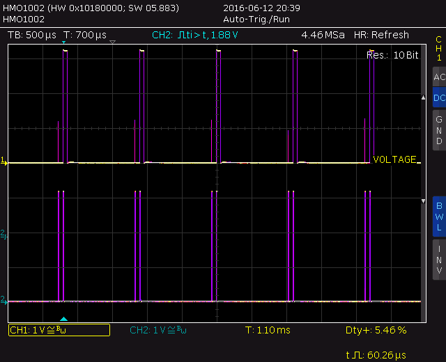
1kHz PWM from Espressif SDK. A specified period of 1 milliseconds results in a period of 1.1 milliseconds.

1kHz PWM from Espressif SDK

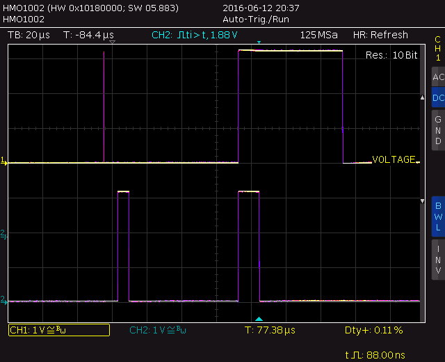
1kHz PWM from Espressif SDK. Each Period is split into a „short pulse“ and a „long pulse“ phase.

As can be seen, in each period typically two pulses are generated, a short and a long one. To calculate the length of the pulses, divide the duty count by (400/3). The integral part is the length of the longer pulse in units of 5.32μs, the remainder is the length of the short pulse. For the given traces:

PWM channel 1
long:  [1467 × 3 / 400] × 5.32μs = 11 × 5.32μs = 58.52μs
short: (1467 – 11 × 400 / 3) × 40ns = (1467 – 1466) × 40ns = 40ns

PWM channel 2
long:  [399 × 3 / 400] × 5.32μs = 2 × 5.32μs = 10.64μs
short: (399 – 2 × 400 / 3) × 40ns = (399 – 266) × 40ns = 5.32μs

From the first trace one can also see that the long pulses run in parallel during the set period of 1000μs, but the short pulses are generated in a fixed size timeslot of 100μs sequentially, i.e. the actual period is 1100μs. Thus the maximum duty cycle is 1000μs (long pulse) + 5.32μs (short pulse) / 1100μs = 91.4%.

For higher PWM frequencies this can be a real problem. When the period is set to 100μs, e.g. 10kHz, the PWM actually runs with 5kHz and the duty cycle is limited to ~50% (Channel 1):

period_100us

10kHz PWM from Espressif SDK. The PWM actually runs at 5kHz, as the right half is not accounted for.

A PWM from scratch

For the reasons stated above, I thought about a new PWM implementation. Requirements were:

  1. Opensource, to be hackable
  2. Usable for 1 to 8 PWM channels
  3. Full 0% to 100% duty cycle
  4. Drop-in replacement for SDK PWM

First thing I learned during the implementation is the quite high interrupt overhead of the NON-OS SDK (same may apply for the xtensa FreeRTOS port) [1]. The interrupt handler which has to be provided to the SDK interrupt attach function is just a normal function (ABI wise), while the lowlevel interupt handler doing the housekeeping, like register saving and dispatching, is hidden somewhere in the ROM. This housekeeping adds about 2.5μs of overhead, which limits the maximum rate for doing timer based interrupts to about 3μs.

So to get a resolution better than 3μs at least part of the GPIO pin toggling has to done with busy loops inbetween. While busy waiting is normally frowned upon, in this case is no worse than interrupts – either way the CPU is busy, either by spinning or by completing the interrupt handler.

Another limiting factor is the access time of the ESP8266 peripheral registers. As others have noted, a write to these registers take about 6 CPU cycles, i.e. 75ns.

Design choices

  1. Mixed interrupt/busy loop concept with single pulse per period
  2. Base interval of 200ns
  3. Phase mirroring for duty cycles above 50%

The third point is the most important one, the one that needs some explanation. A software driven PWM typically enables all active channels at the beginning of the period (t=0) and then one after the other switches the channels off again, depending on the respective pulse width.

For channels with a duty cycle above 50%, these can also be interpreted as having a duty cycle of 100% – duty, but an inverted
polarity. This interpretation allows to remove any switching from the second half of the period, and in turn enables using this timeframe for a more fine granular pulse width generation.

So, how does it look like? Here are 4 PWM chanels, 25kHz PWM period, duty cycle of 45%, 50%, 90% and 2.5% from top to bottom:

4chan_25kHz_2

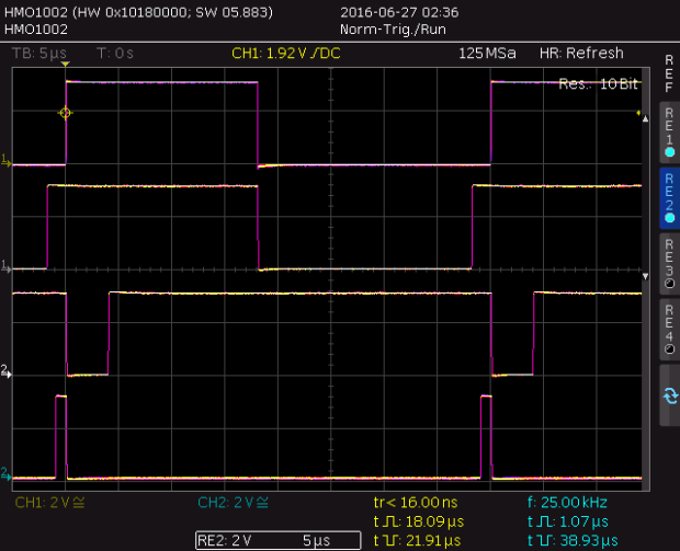
25kHz PWM from new implemantation

Implementation details

The important parts are the actual interrupt handler and the setup routine for the PWM control. Both deal with an array of sequential PWM phases. Each phase switches some GPIOs on and off, and then delays execution until the next phase starts:

struct pwm_phase {
int32_t ticks;
uint16_t on_mask;
uint16_t off_mask;
}

For the 4 channel PWM above, there are 5 phases.

  1.  T= 0us: Enable channel 1, disable channel 3 and 4
  2.  T= 4us: Enable channel 3
  3.  T=18us: Disable channel 1 and 2
  4.  T=38us: Enable channel 2
  5.  T=39us: Enable channel 4

After the first three phases, the timer interrupt is set up for the delay, the last two phases are done with busy waiting inbetween.

The heavy lifting is done in the setup routine called by pwm_start. It sorts channels by duty cycle, aligns PWM pulses to satisfy interrupt rate constraints (as done for channel 1 and 2 here) and transforms the absolut switching times to delays.

The interrupt handler is designed to be as lightweight as possible – it has to be able to switch arbitrary GPIOs every 200ns. To reach this goal, it uses several tricks to minimize instruction count:

  1. Use a struct for related data. This allows the compiler to use relative load with a single base offset for multiple variables.
  2. Use a struct for the GPIO and timer registers. The SDK defines these as independent memory offsets, again combining these into a struct allows to use relative stores.
  3. Do not use the SDK GPIO manipulation macros. These insert a „memw“ (memory wait) instruction, costing two extra cycles (thats 25 precious nanoseconds out of 200 available).

But enough words, code is available here:

https://github.com/StefanBruens/ESP8266_new_pwm

Get some rest or making KDE more power efficient

This article is about saving the world. At least, give our small green planet a chance to last until it is eaten by this red dwarf called sun.

Motivated by an article and my recent purchase of a new laptop, I went looking for some reasons for the mismatch in power usage of KDE vs the other DEs. Although is was not worried about the differences in memory usage (others have commented on measuring memory usage correctly in depth), the increase of power usage between the beginning of the benchmark and the end struck me. As the system is idle in both cases, power usage should be the same, if not, there is something going on.

Weiterlesen

ldapsearch and base64 encoding

ldapsearch is a very nice tool, but there is one small problem — if an attributes value contains any special characters (anything outside the range of printable ASCII characters), the value is base64 encoded.

so for
ldapsearch -x -h abook.rwth-aachen.de -LLL -b o=abook sn='brüns' cn
the results are:
dn: uid=Stefan.Bruens@rwth-aachen.de, ou=datenbank, o=abook
cn:: U3RlZmFuIEJyw7xucw==

the following snippet helps:
alias un64='awk '\''BEGIN{FS=":: ";c="base64 -d"}{if(/\w+:: /) {print $2 |& c; close(c,"to"); c |& getline $2; close(c); printf("%s:: \"%s\"\n", $1, $2); next} print $0 }'\'''

Results:
ldapsearch -x -h abook.rwth-aachen.de -LLL -b o=abook sn='brüns' cn | un64
dn: uid=Stefan.Bruens@rwth-aachen.de, ou=datenbank, o=abook
cn:: "Stefan Brüns"

Warning: Of course this works for attributes with printable characters only. LDAP can contain binary data, e.g. images of the user in JPEG format.

VMware and 3D acceleration on Intel graphics

After this blog has been dead for about two years, I will start with some technical stuff – at least when computers don’t work as expected, most times I know how to fix it.

Ok, lets move on to the topic of this post. Short time ago I was forced to do some stuff on windows again (EEKK — the word registration number still sends me cold shivers …). As I needed really working USB support (unfortunately Nokia thinks Linux is good enough for their hardware, but not for their customers computers), and I was unable to make it work neither in Xen (not at all) nor with KVM (unusably slow), I ended up with VMWare.

So, USB worked really nice, no problems at all. While I was there, I thought „let’s have a look at the 3D acceleration“. At a first glance, it looked quite easy – „upgraded“ the VMs version to 6.5, and ticked the option for „3D acceleration“ – TADA – „Failed to construct 3-D rendering backend. The 3-D features of the display card will be disabled.“

Ok, what’s wrong? After some digging in the log, I found these two suspicious lines:
mks| GLUtil_InstallExtensionLists: Missing required extension GL_EXT_texture_compression_s3tc
mks| GLUtil_InstallExtensionLists: Missing required extension GL_EXT_framebuffer_object

Unfortunately, the Intel driver does not support these two OpenGL extensions – more or less.

Let’s have a deeper look into this. First, S3 texture compression. S3TC is a lossy texture compression used in many games, and it is mandatory for DirectX. Unfortunately, S3TC is covered by some patents, and although the decompression is handled by the hardware, a conformant OpenGL driver has to handle decompression and compression. As in many cases (most games ship with precompressed textures) only decompression is needed, which is handled by the hardware, there is a switch to force Mesa to report support of S3TC although it actually only handles one half – if you want to know more, force_s3tc_enable drirc are the keywords.

If you want to know more, or even want to enable compression as well, have a look at Roland Scheideggers‘ page.
As said, S3TC is covered by patents, so enabling compression is legally problematic. But there may be some hope, as S3TC is „owned“ by VIA, and they recently open sourced their Linux graphics driver, maybe we will even get S3TC out of that – at least, they could put compression under a liberal license, and still sell licenses to ATI/Nvidia/Intel (I still may have some dreams, don’t I?)

The other part is GL_EXT_framebuffer_object, shortly referred to as FBOs. These are really not supported by the Intel driver at the moment, but there the new memory managers come to the rescue, see this post.

Summarized, as soon as GEM has landed in the kernel tree (and/or in the downstream distributions), it should be possible to make it work. GEM should be available soon™, and S3TC can be worked around today.